|
The following images show you some screen dumps from BitScope capturing real waveform data showing how various ADC modules behave under similar circumstances.
ADC5540 @ 25 MHz
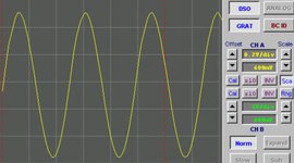
800 kHz Sinewave ~1Vpp
|
This trace shows good linearity and low noise.
|
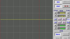
Least sensitive range, no signal
|
ADC shows typical tendency to flip between adjacent states. This looks like noise, but it is the resolution of the 8 bit converter.
|
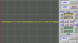
Most sensitive range, no signal
|
High gain range (+/-130mV). From the previous trace of the 3V range, it can be seen that noise at the ADC itself is less than 1 bit. This trace therefore shows the noise floor in the BitScope input stage - about 3mVpp - which is just over 1% FS.
|
ADC5540 @ 40 MHz
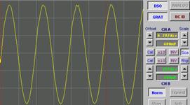
800 kHz Sinewave ~1Vpp
|
|
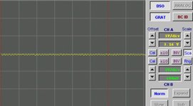
Least sensitive range, no signal
|
|
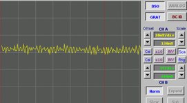
Most sensitive range, no signal
|
Module performance is slightly degraded by clocking it at the 40MHz rate. This is a characteristic of these semi-flash converters - their performance is a function of clock rate and input frequency.
|
EXAR8786 @ 25 MHz
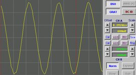
800 kHz Sinewave ~1Vpp
|
This trace shows that the EXAR converter begins to lose ENB at 25MS/S
|
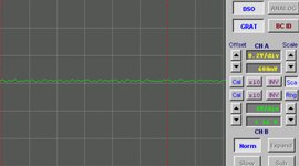
±3V range, no signal
|
Low level noise in EXAR converter is scaled according to range. About 2% FS shows up as 100mV noise on this range. In any 8 bit DSO, this scaled noise needs to be allowed for.
|
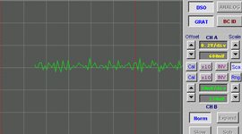
Most sensitive range, no signal
|
Exar converter exhibits about double the noise figure of the new ADC5540 ADC - 6mVpp or 2.3% FS. On this range a small component of the noise is due to the DIP PCB module which can not be shielded as well as the new SMT assembly.
|
MC10319 @ 25 MHz
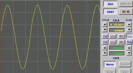
800 kHz Sinewave ~1Vpp
|
|
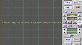
±1V range, no signal
|
|
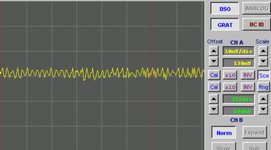
Most sensitive range, no signal
|
The Motorola chip is subject to more noise than the TI5540. Some of this is the digital switching noise caused by the bipolar technology and higher currents operating in the chip.
|
|