The new ADC module gives you the option of sampling data at 40 MHz. BitScope is normally configured to drive the ADC at 25 MHz and must be modified to run at 40 MHz. However, before you leap in and do this, you may wish to consider some of the trade-offs.
Aperiodic Waveform Capture
If the signals you are interested in are periodic, then sub-sampling allows you to measure frequencies beyond 70 MHz running the ADC at only 25 MHz. Indeed, for reasons described below it is preferable to run the ADC at this lower rate.
However, if you wish to capture aperiodic waveforms or one-shot events, and the frequency content of these signals is greater than 12 MHz (ie, half the 25 MHz sample rate), then running the ADC at 40 MHz will allow you to see frequency components up to 20 MHz.
Converter performance
The ADC5540 converter performance varies with sample clock frequency. A close look at the data sheet shows that the ADC begins to lose ENB (effective number bits) when clocked at its maximum rate. This shows up as nonlinearity (noise) imposed on the signal which increases with input frequency.
Some real-world examples demonstrate the difference...
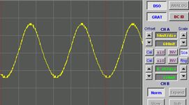
ADC @ 25 MHz - 100 MHz Sinewave ~300mVpp
|
This trace shows the ADC is capable of sampling a 100MHz sinewave using the sub-sampling technique discussed earlier. There is some noise evident and the signal is attenuated due to the very high frequency of the input signal.
|
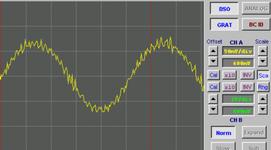
ADC @ 40 MHz - 70 MHz Sinewave ~300mVpp
|
Another sinewave, now sampled at 40 MHz, exhibits more noise. This is due to the lower ENB and slightly increased jitter resulting from the clock doubler circuit. Large signal performance is not affected, however so you will need to consider which is more important to you.
|
Memory Usage
Another issue is sample memory usage. A 40 MS/s BitScope will consume sample RAM twice as fast and limit the maximum capture to about half. Alternatively, if you normally capture less than a full buffer of data, running at 40 MS/s means you will generate up to 2 times as much data which will slow the serial link upload time.
Logic Analysis
If you plan to use BitScope as a high speed logic analyzer with simultaneous analogue signal capture, you may want to run the clock at 40 MHz. This will allow you to capture logic transitions at almost twice the speed of the standard BitScope.
Modifying BitScope for 40 MS/s
BitScope is capable of being clocked at up to 50MS/s limited by the PLD, SRAM, and the PIC microcontroller. The 40 MS/s limit described here is due to the ADC module, and the standard 80 MHz PLD and 15 ns SRAM components. If you are not interested in analogue data capture (ie, you're not using an ADC), you can in fact clock BitScope at 50 MS/s for use as a very high speed logic analyzer if you use a 100 MHz PLD, 12 ns SRAM and omit the ADC.
To run BitScope at 40 MS/s you have two choices; either install an 80 MHz OSC module to replace the standard 50 MHz part, or enable the clock doubler circuit and use a 40 MHz OSC module.
The following notes detail a board level modification to BitScope which should only be attempted by an experienced person. Desoldering components from a multilayer card must be done carefully with appropriate tools to avoid damaging the PCB.
- Install and test ADC5540 module at 25MHz.
- Insert ADC5540 module in 24 pin socket, observing Pin 1
- Make sure 3 pin header (above ADC) is 1-2 OPEN, 2-3 SHORTED
- Set SPAN (RV2) so TP3-TP4 is 1.0V
- Set ADC midpoint (RV1) so TP5-TP4 is 0.0V
- Remove D5, D6 to use ADC5540 clipping circuits. (cut the leads at one end is OK)
- If not using the clock doubler circuit (default).
- Remove U19 50MHz OSC module
- Install 80MHz OSC module in U19
- If using the clock doubler circuit (advanced).
- Remove U19 50MHz OSC module
- Install 40MHz OSC Module in U19 - test this configuration (20MS/s capture rate)
- Remove shorting link at C54 (20pF)
- Install C54 - 22pF
- Install R11 220R nominal, 150R - 330R possible range (optionally adjust for best results at 40MS/s)
Notes
- The new ADC has pin 1 clearly marked - make sure it is inserted correctly!
- If you upgrade to 40MHz using the 80MHz OSC module, it is not easy to go back. Only do this mod if you are confident in your technical abilities.
- If you use the 40MHz clock doubler circuit, you can revert to a non-doubled clock by shorting C54. This will allow you to operate at 40MS/s or 20MS/s without too much trouble.
- The clock doubler relies on C54 and R11 to act as a delay line for the second XOR gate input. The gate characteristics of the AC86 device you use may affect this operation slightly. To get the best x2 clock from the XOR gate may require altering R11 a little either way. This may reduce clock jitter and give better ADC performance at 40MS/s.
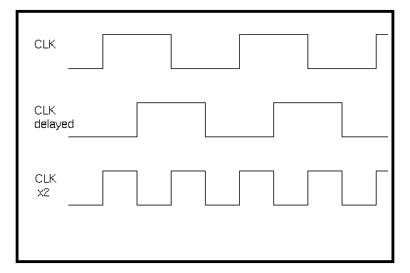
How the clock doubler works
Normally, BitScope uses a x2 Oscillator module with a synchronizing flip-flop to generate zz-clk (the sample clock). To allow more commonly available OSC modules to be used at sample rates of 40MHz (80MHz OSC), a simple clock doubler circuit is included in the BitScope design. This circuit is normally disabled, but can be activated by adding an RC filter.
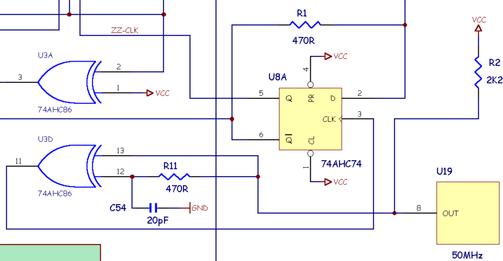
BitScope clock circuit
Refering to the schematic above:
- With C54 shorted and R11 omitted, U3D simply buffers the OSC module.
- With C54 and R11 in place, the signal at U3D/12 is a delayed version of the signal at U3D/13
- U8A generates a synch clk (zz-clk) which is half the freq of the signal at pin 3
The XOR timing diagram below shows how a x2 clock is generated.