| Designs |
|
The original BitScope used a Lattice PLSI1016 PLD to implement the capture engine. We call it Spock and it "soaks up" a lot of logic and makes the circuit look much simpler than it really is. It implements the equivalent of 16 to 20 medium density TTL devices. 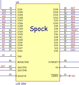
Spock performs two functions: (1) Address generation for the SRAM capture buffers, and (2) 8 bit pattern matching for trigger generation. It is driven by the zz-clk signal and operates in one of two modes: COUNT mode (RB4 low): counter enabled and comparator monitoring the byte stream for trigger matches. SHIFT mode (RB4 high): counter shifting in bits from A-DATA (RB0), and shifting out bits to SEL0 (RB1). We can reload the counter and find out where it was up to when we stopped it. Bits from the top of the counter are also shifted up to the comparator circuits to load the trigger. Spock is connected to the three internal busses in BitScope:
Full details of Spock's functional operation are available here. |
||||||||||||||||||||||||
Copyright © 2023 BitScope Designs


