|
The primary source of analog signals is through the CH A and CH B BNC connectors. 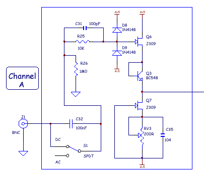
These input circuits are designed to be compatible with normal 10:1 CRO probes. This schematic left shows CH A. CH B is identical. S1 provides AC/DC coupling via 100nF cap C32 and the 1M resistor to GND provides the nominal 1M input impedance. R25, C31, D8 and D9 and provide input protection. The high impedance voltage follower circuit use JFETs Q6 and Q7. The Opperating point and offset adjust is set by Q3/RV3. MAXIM to the rescueJFETs have quite a high output impedance so U23, a unity gain follower, is provided to buffer the analog signal to the next stage. 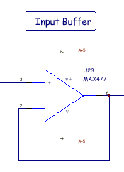
Of course, this buffer and others that follow it must perform to the highest standards if the integrity of the analog signal is to maintained until it reaches the A/D convertor. A few years ago, wide bandwidth OP Amps were considered rocket science. Then came the Maxim MAX477. This device has a 300 MHz GBP, uses voltage feedback and is happy to drive 50 ohm capacitive loads. As an added bonus, it has a 1 Meg input impedance and negligible input capacitance. This is just the ticket for getting a wide bandwidth signal to an A/D convertor. The analog path to the A/D convertor passes through a series of these wide bandwidth OP amps before being applied to 4:1 analog multiplexer. This combination avoids RC filters which could degrade the high frequency components of our signal. Logic POD Analog InputsThe other analog inputs connect via the POD and are attenuated by the 20K network R22 and R23. 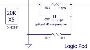
The schematic left shows CH B. CH A is identical. To compensate for the input capacitance of the multiplexer which follows this circuit, an optional speedup capacitor C57 is available. This may need to be trimmed and should have a nominal value of Cin/4 (about 0-10pF). The maximum input voltage of the range buffer which follow this is ±3V. So given an attenuation factor of 4.830, this means a maximum analog voltage at the POD of ±15V can be measured. This is suitable for most solid state designs. Higher voltage ranges can be accomodated with extra circuitry in the POD itself. |
Copyright © 2023 BitScope Designs


