|
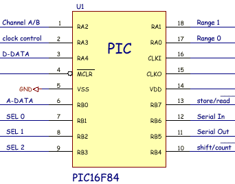
The original BitScope is based on the MicroChip PIC 16F84 we call Picard.
Its fast RISC instruction set and the tri-state I/O pins make it ideal for BitScope.
At first glance you may think that an 18 pin PIC does not have enough pins for a useful design.
However, with careful planning it is possible to use most pins for more than one function which makes good use of the features of this innovative microcontroller while keeping the construction costs down.
The key is to reuse several of the pins depending on the hardware operating mode. In BitScope's case, two modes are defined; COUNT and SHIFT.
Here is a brief description of the pin functions:
| PIN |
Function |
Description |
|
RA0
RA1 |
Range 0
Range 1 |
COUNT mode:
Output pins that control the Analog gain of the Y amplifiers.
- 0 Gain = 4.583
- 1 Gain = 1.000
- 2 Gain = 0.500
- 3 Gain = 0.190
Note that the gain of the ADC Buffer is 1.667
|
|
POD I/O 0
POD I/O 1 |
SHIFT mode:
I/O pins that are available at the LOGIC POD for
external Smart Ports. In COUNT mode, analog switches
isolate these signals from the LOGIC POD.
|
|
| RA2 |
Channel A/B |
Output pin that swiches the Analog source between CHA BNC and CHB BNC,
or in POD mode between PODA or PODB analog signals brought from the LOGIC
POD.
|
|
| RA3 |
zz-clk |
"The clock that sleeps". Tri-state I/O pin. State
machines in PLD devices should not be exposed to glitches
on the clock. Some registers may see the clock, others may
may not, resulting in non-deterministic behavior. Jamming
a 50MHz clock signal is not polite. U6A (74AC74) is double
clocked by frequency doubler U3D (74AC86) (on the clean
edge) and allows the PIC to have 3 state synchronous
control via RA3. High, Low, Freerunning - no
glitches. This control is important as we must use zz-clk
to shift in control words to the PLD as well as modulate
the sampling for lower frequency timebase measurements.
|
|
| RA4 |
Digital Data |
Input connects to U5 8:1 MUX to read the 8 data bits of
the Logic Analyzer RAM bus. Bit7 is routed through Spock
to be optionally the TRIGGER MATCH or FREQUENCY/EVENT
signals. RA4 may be connected to the PIC prescaler in the
OPTION register
|
|
| RB0 |
Analog Data |
COUNT mode:
Input connects to U4 8:1 MUX to read the 8 data bits of
the ADC RAM Bus. As RB0 is the PIC INT source, during
SAMPLE, if the MUX points to Bit7 then INT may be used as
a zero crossing detector for Analog TRIGGER (in additional
to the Complex trigger implemented in the PLD)
|
|
Spock Data In |
SHIFT mode:
Output signal is Shift-In data to feed Spock which needs 5 bytes to
set up counters, trigger bytes and options.
|
|
| RB1 |
SEL 0 |
COUNT mode:
Output A0 for data MUXs U4, U5.
|
|
Spock Data Out |
SHIFT mode:
Input Shift-Out data from Spock. Current 16 bit counter
state in Spock is shifted out as new data is shifted in.
|
|
RB2
RB3 |
SEL 1
SEL 2 |
Output pins A1, A2 for data MUXs U4, U5.
|
|
| RB4 |
COUNT/!SHIFT |
Output which controls the hardware mode. That is, COUNT or
SHIFT. A value of ONE causes Spock to shift new data into
its registers. A value of zero causes Spock to count and
trigger.
|
|
| RB5 |
Serial Out |
Serial data output.
|
| RB6 |
Serial In |
Serial data Input.
|
|
| RB7 |
STORE/!READ |
Output control for RAM and ADC/Buffer control. This signal
selects either read or write for the RAM, allowing SAMPLE
data written to RAM, or later read back.
|
|
CLKI
CLKO |
Clock Select |
The PIC is clocked by a crystal - which depending on the PIC device
may be 4MHz, 10 MHz or 20MHz
|
|


